_roibu_Alamy.jpg?width=1280&auto=webp&quality=80&disable=upscale#)


![Apple Slips to Fifth in China's Smartphone Market with 9% Decline [Report]](https://www.iclarified.com/images/news/97065/97065/97065-640.jpg)
![EU Postpones Apple App Store Fines Amid Tariff Negotiations [Report]](https://www.iclarified.com/images/news/97068/97068/97068-640.jpg)

![New Beats USB-C Charging Cables Now Available on Amazon [Video]](https://www.iclarified.com/images/news/97060/97060/97060-640.jpg)


![Beats showcases Android in ad for ‘universally compatible’ cables that Apple was forced to support [Video]](https://i0.wp.com/9to5google.com/wp-content/uploads/sites/4/2025/04/beats-cables-4.jpg?resize=1200%2C628&quality=82&strip=all&ssl=1)


![[The AI Show Episode 144]: ChatGPT’s New Memory, Shopify CEO’s Leaked “AI First” Memo, Google Cloud Next Releases, o3 and o4-mini Coming Soon & Llama 4’s Rocky Launch](https://www.marketingaiinstitute.com/hubfs/ep%20144%20cover.png)


Design a Lattice FPGA HDMI Transmission Scheme
Here's a comprehensive Lattice FPGA HDMI Transmission Scheme design using low-power Lattice FPGAs (e.g., ECP5 or CrossLink-NX). This solution covers hardware, FPGA logic, and software components for robust HDMI signal transmission: 1. System Overview Target Devices: Lattice ECP5 (for cost-sensitive designs) or CrossLink-NX (for embedded MIPI DSI/CSI-to-HDMI bridging) HDMI Version: 1.4b (Supports 1080p60, with optional TMDS scrambling for EMI reduction) Key Features: TMDS Signal Generation (FPGA-native or external PHY) EDID Management (Hot-Plug Detect, DDC I2C) Color Space Conversion (RGB ↔ YCbCr 4:4:4) Audio Embedding (I2S to HDMI Audio Packet) 2. Hardware Design A. Block Diagram [Video Source] → [Lattice FPGA] → [HDMI Transmitter] → [HDMI Connector] (ECP5/CrossLink) (e.g., IT66121 or native TMDS) B. Critical Components FPGA Selection: ECP5-85F (For 1080p60 with internal LVDS→TMDS conversion) CrossLink-NX-17 (For MIPI DSI/CSI to HDMI conversion) HDMI PHY Options: Internal TMDS (ECP5 LVDS pins + SERDES) External PHY (e.g., IT66121 for simplified design) Clock Architecture: 148.5 MHz for 1080p60 (Pixel Clock) 27 MHz for I2C/EDID management Optional PLL for audio clock (e.g., 12.288 MHz for 48kHz audio) Connectors: HDMI Type A (Standard 19-pin) ESD Protection (TVS diodes on TMDS lines) 3. FPGA Logic Design (Verilog/VHDL) A. TMDS Encoder Core verilog module tmds_encoder ( input clk_pixel, input [7:0] data, input [1:0] control, output [9:0] tmds ); // Implement DVI 1.0 Spec TMDS encoding // Includes XOR/XNOR reduction and DC balancing endmodule B. Video Timing Controller verilog module video_timing ( output [11:0] h_count, output [11:0] v_count, output h_sync, v_sync, data_enable ); // Generates 1080p60 timing: // Active: 1920x1080, Front Porch/Sync/Back Porch endmodule C. I2C EDID Handler verilog module edid_reader ( inout sda, output scl, input hpd, output [7:0] edid_data ); // Responds to DDC requests and serves EDID // Implements I2C slave at address 0x50 endmodule 4. Software Components A. Lattice Diamond/Primary Configuration Pin Constraints (.lpf file for ECP5): LOCATE COMP "tmds_clk_p" SITE "E4"; IO_TYPE "LVDS25"; PLL Configuration: Generate 148.5 MHz from 25 MHz oscillator Phase-align TMDS clock/data B. Embedded RISC-V Core (For Smart HDMI) Use Lattice Propel to add soft-core CPU for: EDID parsing Dynamic resolution switching Audio packet generation 5. Signal Integrity Considerations PCB Layout Rules: TMDS Differential Pairs: 100Ω impedance, length-matched (±50mil) Layer Stackup: Route on adjacent layers with ground plane Termination: On-die termination (ODT) in ECP5 EMI Reduction: Enable TMDS scrambling (HDMI 1.3+) Spread-spectrum clocking (if supported by sink) 6. Testing & Validation Test Pattern Generator: Implement color bars/ramp in FPGA logic verilog case (h_count[3:0]) 0: {r,g,b} = 8'hFF; // White 1: {r,g,b} = 8'h00; // Black // ... Color pattern endcase Compliance Testing: Use HDMI analyzer (e.g., Quantum Data) Verify: TMDS eye diagram EDID response time (
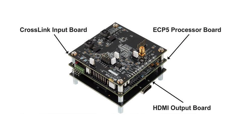
Here's a comprehensive Lattice FPGA HDMI Transmission Scheme design using low-power Lattice FPGAs (e.g., ECP5 or CrossLink-NX). This solution covers hardware, FPGA logic, and software components for robust HDMI signal transmission:
1. System Overview
Target Devices: Lattice ECP5 (for cost-sensitive designs) or CrossLink-NX (for embedded MIPI DSI/CSI-to-HDMI bridging)
HDMI Version: 1.4b (Supports 1080p60, with optional TMDS scrambling for EMI reduction)
Key Features:
- TMDS Signal Generation (FPGA-native or external PHY)
- EDID Management (Hot-Plug Detect, DDC I2C)
- Color Space Conversion (RGB ↔ YCbCr 4:4:4)
- Audio Embedding (I2S to HDMI Audio Packet)
2. Hardware Design
A. Block Diagram
[Video Source] → [Lattice FPGA] → [HDMI Transmitter] → [HDMI Connector]
                   (ECP5/CrossLink)   (e.g., IT66121 or native TMDS)
B. Critical Components
- FPGA Selection:
- ECP5-85F (For 1080p60 with internal LVDS→TMDS conversion)
- CrossLink-NX-17 (For MIPI DSI/CSI to HDMI conversion)
- HDMI PHY Options:
- Internal TMDS (ECP5 LVDS pins + SERDES)
- External PHY (e.g., IT66121 for simplified design)
- Clock Architecture:
- 148.5 MHz for 1080p60 (Pixel Clock)
- 27 MHz for I2C/EDID management
- Optional PLL for audio clock (e.g., 12.288 MHz for 48kHz audio)
- Connectors:
- HDMI Type A (Standard 19-pin)
- ESD Protection (TVS diodes on TMDS lines)
3. FPGA Logic Design (Verilog/VHDL)
A. TMDS Encoder Core
verilog

module tmds_encoder (
  input clk_pixel,
  input [7:0] data,
  input [1:0] control,
  output [9:0] tmds
);
  // Implement DVI 1.0 Spec TMDS encoding
  // Includes XOR/XNOR reduction and DC balancing
endmodule
B. Video Timing Controller
verilog

module video_timing (
  output [11:0] h_count,
  output [11:0] v_count,
  output h_sync, v_sync, data_enable
);
  // Generates 1080p60 timing:
  // Active: 1920x1080, Front Porch/Sync/Back Porch
endmodule
C. I2C EDID Handler
verilog

module edid_reader (
  inout  sda,
  output scl,
  input  hpd,
  output [7:0] edid_data
);
  // Responds to DDC requests and serves EDID
  // Implements I2C slave at address 0x50
endmodule
4. Software Components
A. Lattice Diamond/Primary Configuration
- Pin Constraints (.lpf file for ECP5):
LOCATE COMP "tmds_clk_p" SITE "E4";
IO_TYPE "LVDS25";
- PLL Configuration:
- Generate 148.5 MHz from 25 MHz oscillator
- Phase-align TMDS clock/data
B. Embedded RISC-V Core (For Smart HDMI)
Use Lattice Propel to add soft-core CPU for:
- EDID parsing
- Dynamic resolution switching
- Audio packet generation
5. Signal Integrity Considerations
- PCB Layout Rules:
- TMDS Differential Pairs: 100Ω impedance, length-matched (±50mil)
- Layer Stackup: Route on adjacent layers with ground plane
- Termination: On-die termination (ODT) in ECP5
- EMI Reduction:
- Enable TMDS scrambling (HDMI 1.3+)
- Spread-spectrum clocking (if supported by sink)
6. Testing & Validation
- Test Pattern Generator:
Implement color bars/ramp in FPGA logic
verilog

case (h_count[3:0])
  0: {r,g,b} = 8'hFF; // White
  1: {r,g,b} = 8'h00; // Black
  // ... Color pattern
endcase
- Compliance Testing:
Use HDMI analyzer (e.g., Quantum Data)
Verify:
- TMDS eye diagram
- EDID response time (<200ms)
- Hot-plug detection
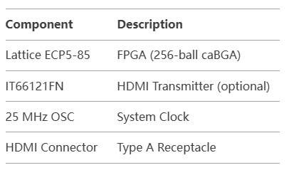
7. Example Implementation (ECP5-85F)
Bill of Materials
Resource Utilization (Estimate)
- Logic Cells: ~5k LUTs (for 1080p60)
- Memory: 2x SPRAM (for line buffering)
- PLLs: 1 (for pixel clock generation)
8. Advanced Features (Optional)
- HDCP Encryption:
- Requires licensed IP core
- CrossLink-NX supports hard-IP HDCP 1.4
- 4K Support:
- Use ECP5-85F with external TMDS buffer
- Requires dual-link HDMI or switch to DisplayPort
- Embedded Audio:
verilog

audio_packetizer u_audio (
  .i2s_data(audio_data),
  .hdmi_header(audio_header),
  .data_island(packet_data)
);
Debugging Tips
- No Signal?:
- Check HPD (Hot Plug Detect) pull-up
- Verify DDC I2C communication with logic analyzer
- Sparkles/Garbled Image:
- Recheck SERDES alignment
- Validate TMDS termination
- Use Lattice Reveal:
tcl

reveal_insert -port h_sync -name h_sync_debug
reveal_trigger -condition {h_count == 0}
This design balances cost, performance, and flexibility. For production designs, consider Lattice's HDMI IP核 or Reference Designs (like the ECP5 Video Interface Kit).