


![Trump Tells Cook to Stop Building iPhones in India and Build in the U.S. Instead [Video]](https://www.iclarified.com/images/news/97329/97329/97329-640.jpg)


![[The AI Show Episode 147]: OpenAI Abandons For-Profit Plan, AI College Cheating Epidemic, Apple Says AI Will Replace Search Engines & HubSpot’s AI-First Scorecard](https://www.marketingaiinstitute.com/hubfs/ep%20147%20cover.png)


![How to Enable Remote Access on Windows 10 [Allow RDP]](https://bigdataanalyticsnews.com/wp-content/uploads/2025/05/remote-access-windows.jpg)


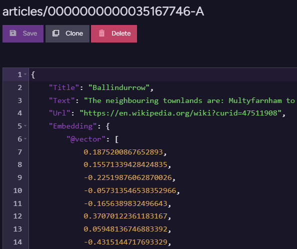


LACED: Peeling Back PCB Layers With Chemical Etching and a Laser
Once a printed circuit board (PCB) has been assembled it’s rather hard to look inside of it, which can be problematic when you have e.g. a multilayer PCB of an …read more
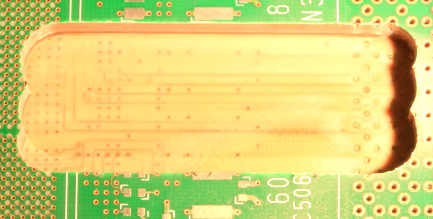

Once a printed circuit board (PCB) has been assembled it’s rather hard to look inside of it, which can be problematic when you have e.g. a multilayer PCB of an (old) system that you really would like to dissect to take a look at the copper layers and other details that may be hidden inside, such as Easter eggs on inner layers. [Lorentio Brodeso]’s ‘LACED’ project offers one such method, using both chemical etching and a 5 Watt diode engraving laser to remove the soldermask, copper and FR4 fiberglass layers.
This project uses sodium hydroxide (NaOH) to dissolve the solder mask, followed by hydrogen chloride (HCl) and hydrogen peroxide (H2O2) to dissolve the copper in each layer. The engraving laser is used for the removing of the FR4 material. Despite the ‘LACED’ acronym standing for Laser-Controlled Etching and Delayering, the chemical method(s) and laser steps are performed independently from each other.
This makes it in a way a variation on the more traditional CNC-based method, as demonstrated by [mikeselectricstuff] (as shown in the top image) back in 2016, alongside the detailed setup video of how a multi-layer PCB was peeled back with enough resolution to make out each successive copper and fiberglass layer.
The term ‘laser-assisted etching’ is generally used for e.g. glass etching with HF or KOH in combination with a femtosecond laser to realize high-resolution optical features, ‘selective laser etching’ where the etchant is assisted by the laser-affected material, or the related laser-induced etching of hard & brittle materials. Beyond these there is a whole world of laser-induced or laser-activated etching or functionalized methods, all of which require that the chemical- and laser-based steps are used in unison.
Aside from this, the use of chemicals to etch away soldermask and copper does of course leave one with a similar messy clean-up as when etching new PCBs, but it can provide more control due to the selective etching, as a CNC’s carbide bit will just as happily chew through FR4 as copper. When reverse-engineering a PCB you will have to pick whatever method works best for you.
Top image: Exposed inner copper on multilayer PCB. (Credit: mikeselectricstuff, YouTube)